
Continued from this article. I’ve done with the phase one experiment.
The goal of phase one experiment is to implement end-to-end application with minimum struggle for hardware design and implementation.
What does the application do?
I am sure there will be a lot of testing work before I put the communication device in real applications. So I first want a tool to test the driver and protocol. Thus, the application for the first phase is a protocol tester that provides command line interface and several diagnostic commands / functions.
Hardware
Arduino was the best for this expriment to develop the software quickly on the ready-made hardware platform.
In this experiment, I avoided adding electrical parts as much as possible and tried to fill missing parts by software.
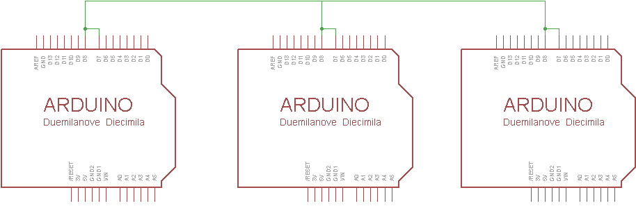
Below is the schematics of the experimental network. An Arduino module works as a communication node. Each connects to a single common bus at digital pins 7 and 8. Pin 7 is used as listener (input) and pint 8 is used for driver (output).
Physical Layer
In order to handle conflict, the bus needs to have two states which are recessive and dominant. Recessive is the idle state. If all devices are recessive, the bus is recessive. If one or more devices are dominant, the bus state is dominant even if some device has recessive driver state. In short, dominant always wins.
In this experiment, the driver is implemented based on following strategy:
- Always set digital 7 pin mode as input, and pull the pin up.
- Always set LOW to digital 8 pin.
- In recessive state, digital 8 pin is input mode, thus pin 8 is disconnected from the bus.
- In dominant state, digital 8 pin is output mode, thus pin 8 is connected to the bus and value is LOW.
In recessive state, the bus is HIGH level. Dominant state is much stronger, so one of the devices has dominant output, bus state becomes dominant which is LOW level.
For implementation, I didn’t use pinMode for switching output state since the function is too slow. Instead, I directly manipulated PORTB bit 0 that is digital 8 pin for Arduino. Also I used PORTD bit 7 to control digital 7 pin.
Here is the implementation of output state control:
setup() {
...
  DDRD &= ~_BV(DD7); // set input mode to PORTD bit 7
  PORTD |= _BV(PORTD7); // pull up
...
}

inline void setDominant()
{
  DDRB |= _BV(DDB0);
}

inline void setRecessive()
{
  DDRB &= ~_BV(DDB0);
}
The Architecture
Following figure shows architecture of phase zero experiment program.

Bus reader and writer take care of communication layers from 1 (physical) to 3 (transport) and the application part takes care of rest. L4 (protocol) is very simple. In this experiment, the protocol is direct translation of packet and there is no session state in this layer. So L4 processor in the test program are just packet creator and reader.
Application part and bus reader/writer part are isolated using read/write buffers. These buffers are the only common places where both parts access. Application part works in the main loop. Bus reader and writer work in interrupt handlers. So update conflict in any data is carefully avoided.
(to be continued…)

 with Arduino UNO")


