DR-110 that I am modifying currently takes 6V power supply from 4 AA batteries or 9V from an AC adapter. But since I’m thinking of connecting to USB, it’s convenient if we can draw power from it. From the device circuit diagram, I found the device requires at least 6V supply although USB supply power is 5V. It’s a good opportunity to learn how to use DC-DC booster since more project that uses USB will come.
I live near Jameco. It’s the best to use one they carry. It’s even better if the package is DIP since I often use breadboards. I checked their catalog and found a switching regulator called MC34063 is cheap and has plenty of inventory. It is versatile, too, that supports boosting, busting, and negating the power supply. I think this is a good choice for my regular switching regulator.
For DR-110, I decided to put 7V that is slightly higher than battery power. The circuit has a simple linear regulator. I expect it removes noise in the switching regulator output as long as it is small. The current supply probably is good enough with 50mA.
Collecting document is necessary first. Jameco provides MC34063 manufactured by STMicro, but their datasheet is simplified and vague. I cannot understand how to use it for lack of knowledge of switching regulator fundamentals. I also found decent application notes from ON Semiconductor and TI sites. They looked to have the same source and the contents look the same.
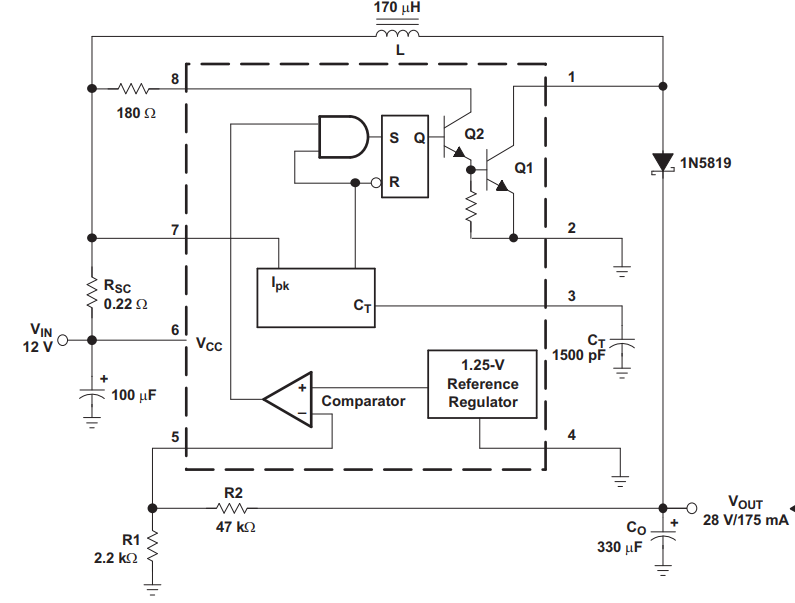
Following is an example circuit diagram of boost regulator. The circuit has a n oscillator that drives switch Q1 and Q2 that draws current from L to accumulate energy to boost power supply. The output voltage is determined by comparator that listens on output and adapts duty cycle of the switch in negative feedback manner. Well, it’s a smart design.
First, I used this circuit as is with modifying only R2 to make 7V output, but it generates a lot of audible ripple noises in the output. This approach was useless. I should took proper way that is to calculate circuit parameters by reading and understanding application notes. The application notes has enough information to design the circuit.
The frequency of the oscillator is determined by CT, and other parts hardly affect it. I decided the frequency first (a little lower than 100 kHz that is highest possible frequency). Then decided the switching duty cycle. Finally decided minimum L value. Tried the circuit using simulator and tweaked the parameters. The diagram below is the designed parameters. The resistor R4 is a load.
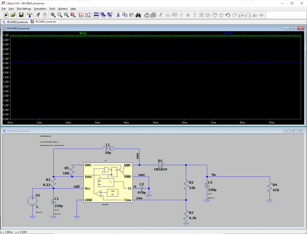
I found one difficulty in designing a switching regulator is that the behavior changes significantly when the load changes. Analog circuit usually does not change its circuit current drastically, so it might be better to figure it out when attaching a switching regulator. Following picture shows the behavior change when the load is very light (100 kΩ). Switching timings are much slower. Slow ripples are clearly visible, which must be so bad to an analog audio circuit. It’s better to experiment with real circuit to proceed further. But I don’t have a 10 μH inductor right now. So that’s it for today.
