
I’ve been building trimless VCA units. The resources are available here:
https://github.com/naokiiwakami/vca-unit/tree/v2
The simulation runs well. Tested the circuits on breadboard, went fine. Built a prototype on a 3″ x 2″ universal PCB, working fine. But the goal size is much smaller – 7/8″ x 3/8″. When I try a PCB of this size, a significant offset appears on output (0.4V to 1V, negative or positive) for zero input with -5V CV. This really puzzles me as all came from the same schematic. Such a large offset causes popping noises with steep CV attacks. I need to eliminate it.
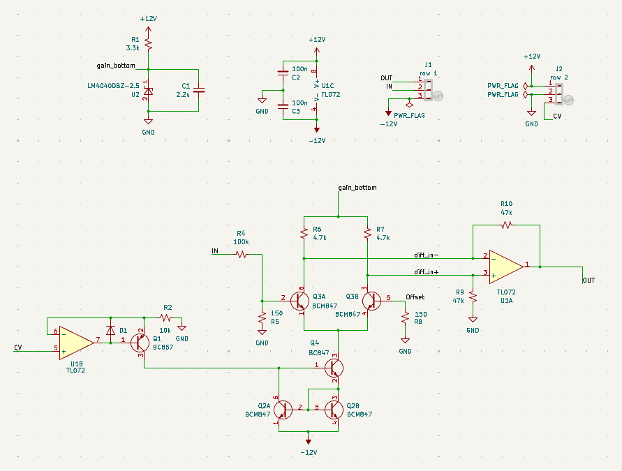
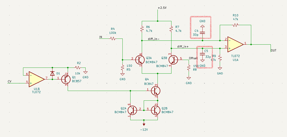
I’m building two types of VCAs in this project; NPN type that takes negative CV and PNP type that takes positive CV. Following is the schematic of the NPN type. I used this type for troubleshooting.
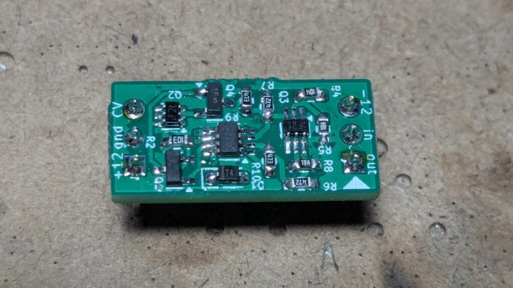
The appearance looks as the following. The components are placed pretty closely.
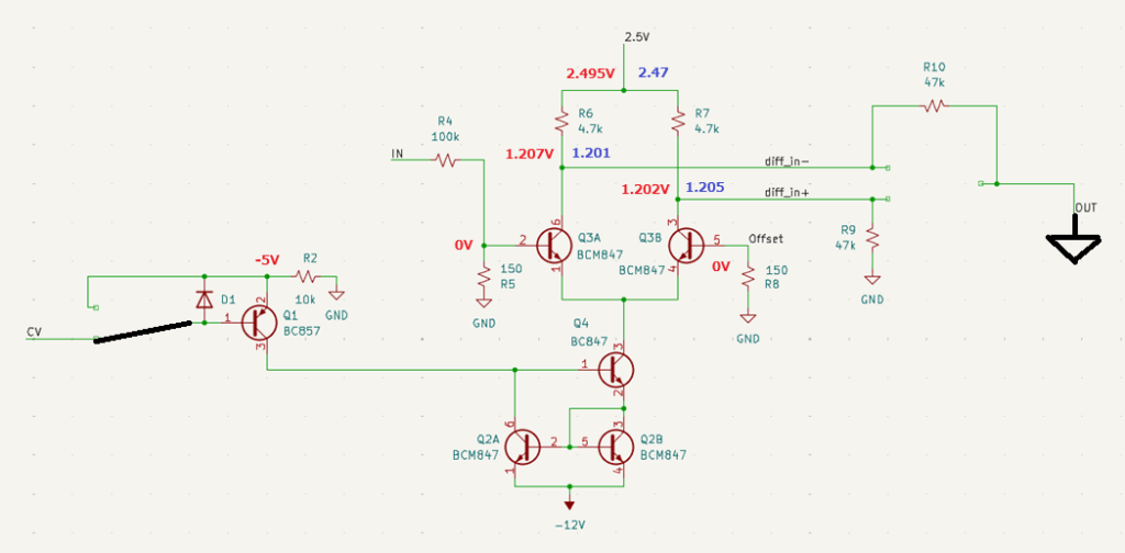
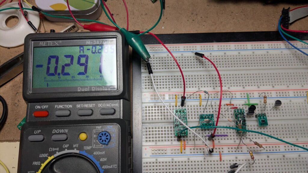
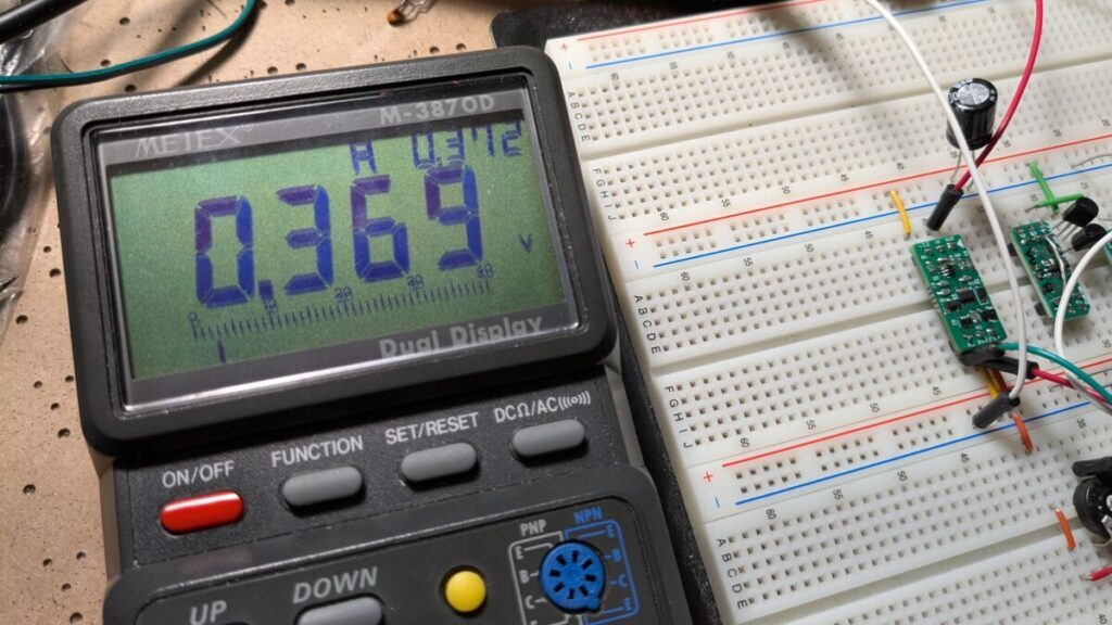
I first took the op amp off from the PCB to see if the gain unit transistors Q3 are matched. I connected the output to the GND so that the Q3 pair is completely symmetric (ignore R4 and IN, it’s kept open). CV input is connected directly to the base of Q1 because the op amp unit for CV-to-current circuit has been removed, too. Current to the Q3 can be controlled in this way still (set -5V CV). Voltages in red are readings on the PCB. I also built another similar circuit on a breadboard and their readings are in blue. Values are close and I expect only about 50mV of offset. I don’t find any significant difference between the PCB and breadboard versions so far.
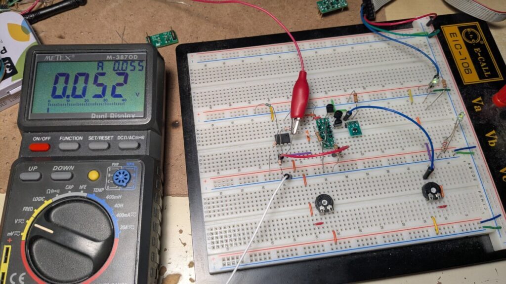
I put the differential amp on the breadboard and the output was around 50mV indeed.
I really don’t understand why this happens. How come the output of the PCB version becomes this big when I put the output diff amp of 10x for 5mV difference?
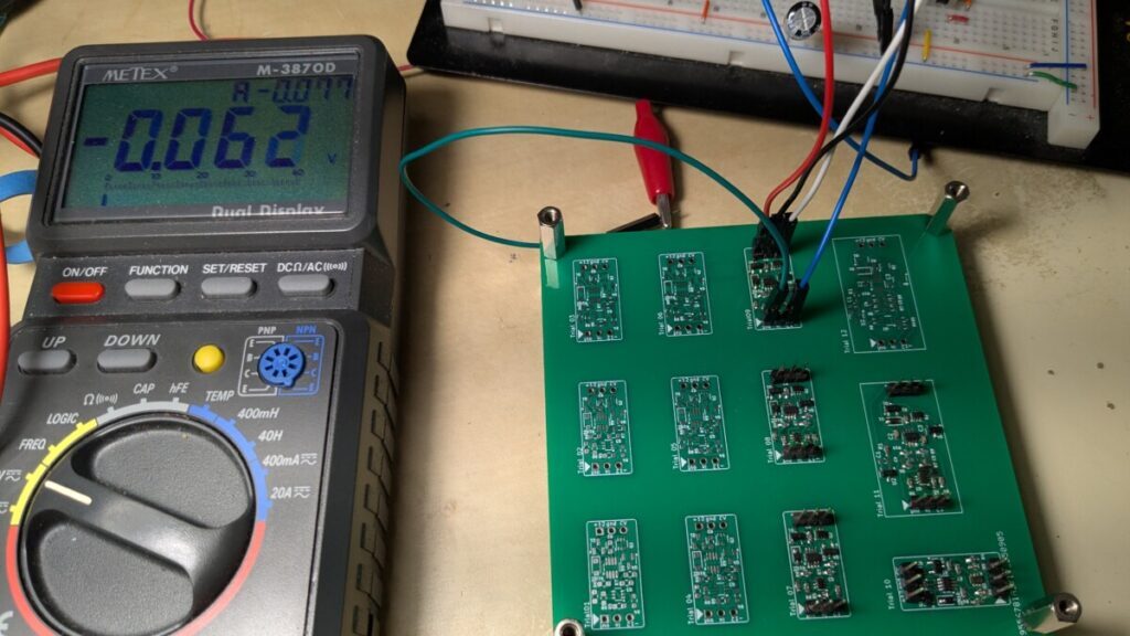
So I built another PCB version piece by piece, borrowing missing parts from breadboard as listed below:
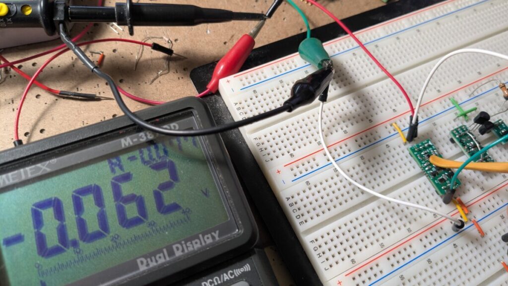
| Output diff amp | 2.5V voltage source | CV to current | Gain unit (Q3) | Offset |
|---|---|---|---|---|
| breadboard | breadboard | breadboard | breadboard | fine (~50mV) |
| breadboard | PCB | breadboard | breadboard | fine (~50mV) |
| breadboard | PCB | PCB | breadboard | fine (~50mV) |
| PCB | PCB | PCB | breadboard | fine (~50mV) |
| breadboard | PCB | PCB | PCB | fine (~50mV) |
| PCB | PCB | PCB | PCB | bad offset (-0.4V) |
This does not make sense to me. The bad offset appear only when all components are on the PCB and it does not happen when one of the pieces is outside?
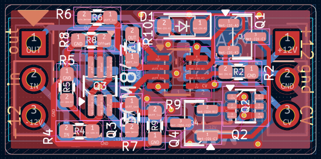
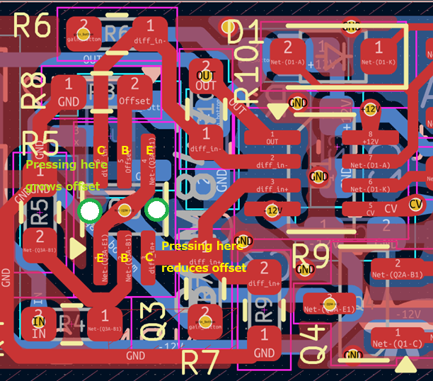
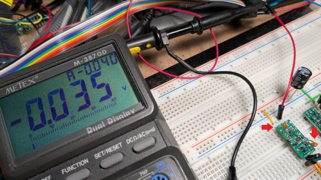
I also noticed when I was playing around the PCB that the offset changes drastically from -0.4V to tens of millivolts when I press the Q3 hard by a bamboo stick. It’s not some electrical effect as Bamboo does not conduct electricity. So is it a mechanical effect? Is the component extremely sensitive to some distance? I still have no idea. It’s not because of bad soldering. I suspect it first and checked ten times.
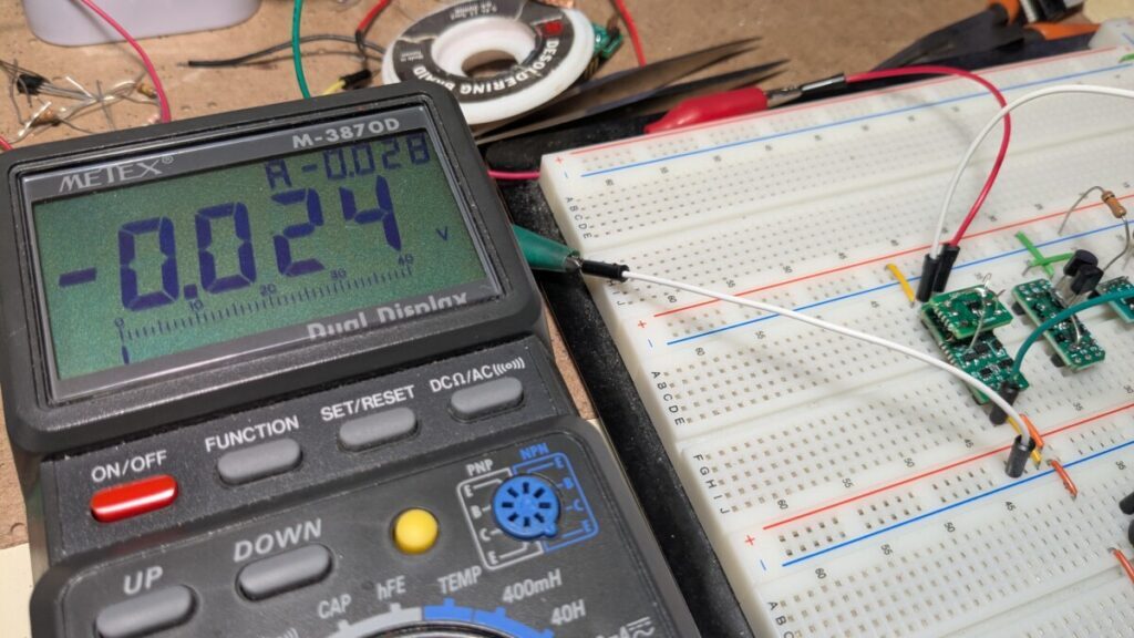
But this gave me some clue. I wonder if the circuit works correctly when the Q3 takes some distance from the PCB. I hanged it above the PCB to see it.
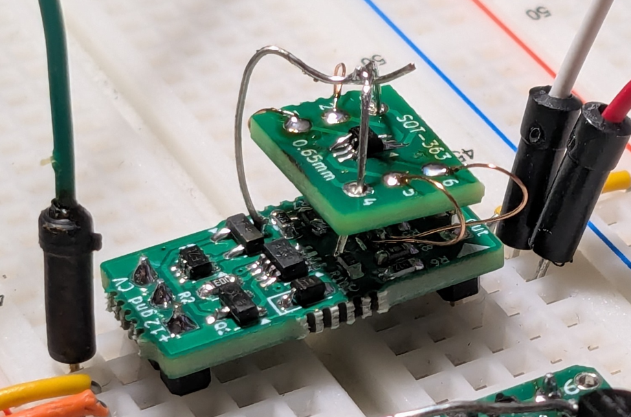
The result is… fine now
OK I finally found a way to eliminate the bad offset. But the solution is far from realistic. I have to modify the PCB design to eliminate this problem.
I suspect too tight routs causes misbehavior in some semiconductor, but couldn’t figure out the theory for it yet. The troubleshooting continues.
Edit: 9/1/2025
As I ran out of ideas, I asked about this issue to the synth-diy mailing list and a Japanese synth builders’ community. Thankfully, several people gave me advices. Some suggest hidden capacitance and oscillation. I initially thought it was not the case since I didn’t find a significant oscillation by oscilloscope. But some of my observations also suggest existence of hidden capacitance and oscillation, such as
- Putting a finger on the gain unit transistor changes the offset drastically
- The offset even changes by pressing the transistor by a bamboo stick (I presume some capacitance changes)
- The offset starts from almost zero on power up, then it grows to ~0.4V slowly (it usually happens when a large capacitance exists which is not the case or the circuit oscillates)
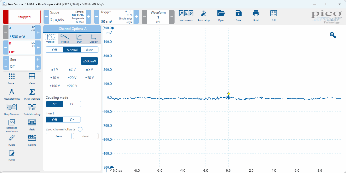
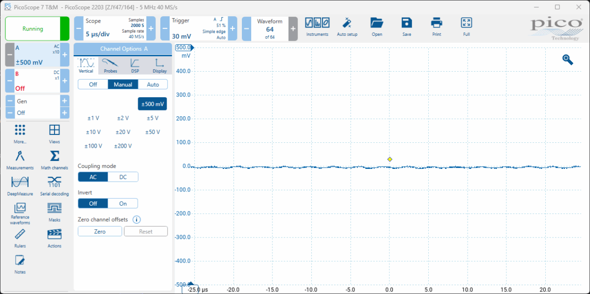
So I put my oscilloscope to the output again. I overlooked when I did it last time, but there seems some tiny oscillation. The amplitude looks like 10-20mV peak to peak, but it may be actually larger because my oscilloscope’s bandwidth is relatively narrow (5MHz) and the oscillation may be happening at higher frequency.
I looked for any possible hidden capacitance. Offset change by pressing the gain unit transistor might be a clue. The behavior is asymmetric. From this behavior, I suspect some capacitance between collectors and somewhere (GND?) contributes to the oscillation.
I tried putting 33pF to the differential amp inputs to balance them by larger capacitors than hidden ones as the following schematic
then the oscillation stopped.
The offset also went down to a reasonable level.
But the behavior is still pretty unstable. I couldn’t duplicate this fix by replacing the capacitors by SMD ones.
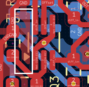
There is another concern. A plated ground is placed very closely to the gain unit transistors on the front side which may create some hidden capacitance asymmetrically.
To see if this plate affects the behavior, I removed it from a PCB and built another unit using it.
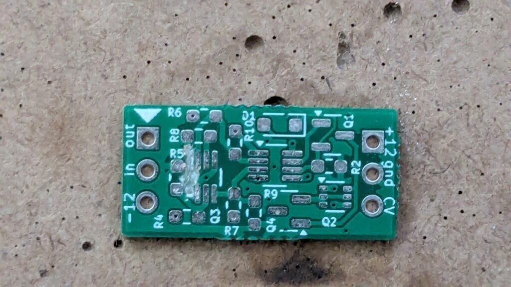
The result is more drastic than I expected although the offset is not under control yet. The polarity of the offset reversed and the offset does not change by pressing the transistor anymore.
I have not figure out the theory yet, but I should try much more symmetric routing below the transistors.
Edit: 10/29/2025
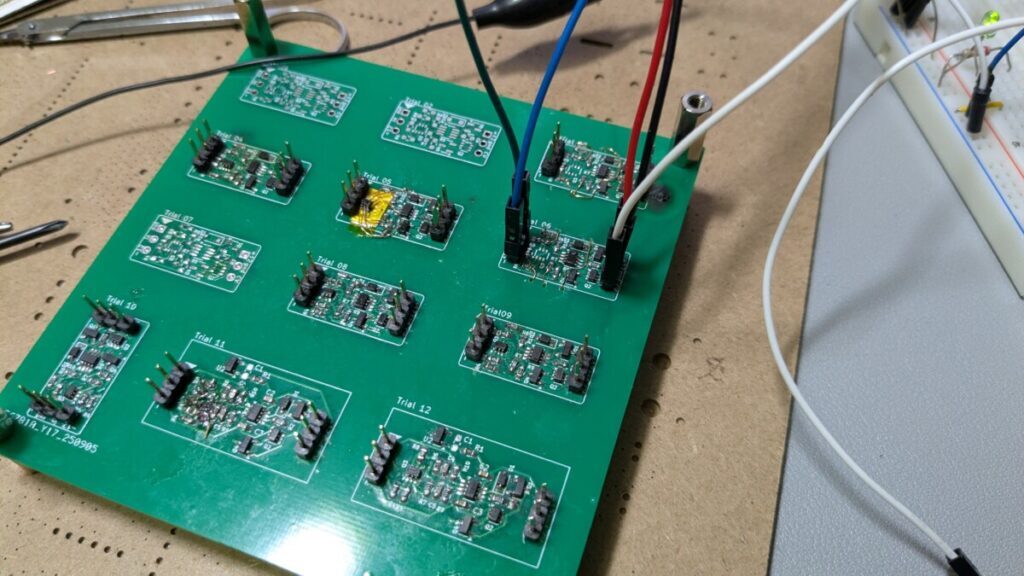
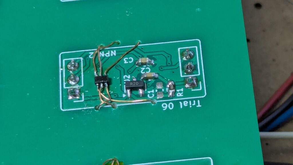
I created a PCB that contains multiple versions of VCA units where I applied fixes blindly (as I don’t know for sure what improves the offset). Some versions show better offsets, but I like to have a little better offset since errors in resistor values and transistor mismatch may push the offset a little further.
I’m planning to run another round of trials by making similar PCB. But I want to have more confidence before doing so. So I started modifying current PCB to do several more trials.
I finally got the result that I consider good enough.
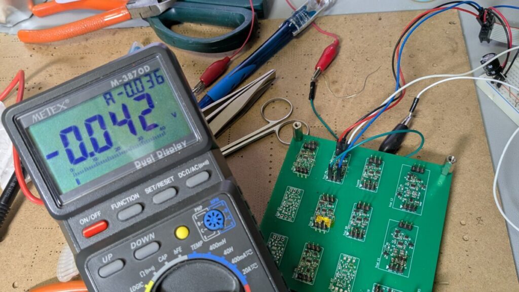
The one that has plated ground on the back side and the gain unit transistors on top of the plate showed the best result. Decoupling the gain unit transistors and the op amp for differential amp electrically seems the key. But I still cannot figure out the theory behind it.
Designing the PCB from this result is still challenging, but I feel I climbed one step above and harnessed myself.


